
System in Package Technology & Manufacturing
Advanced packaging expertise for multi-chip integration, miniaturization, and industrial-grade reliability
Embedding more functionality into smaller form factors while maintaining industrial-grade reliability requires advanced packaging technology. Whether you're designing IoT sensors, automotive control units, or secure authentication devices, integrating multiple chips, passive components, and sensors into a single package determines whether your product succeeds or fails in harsh environments.
Traditional approaches using separate components on a PCB consume board space, add interconnection failures, and limit operating temperature ranges. For applications requiring extended temperature operation (-40°C to +85°C), high shock and vibration resistance, or long-term supply availability (10-15 years), conventional packaging falls short.
System in Package (SiP) technology solves this by integrating multiple bare dies, passive components, and sensors into a single, robust module. Swissbit controls the complete SiP value chain in Berlin - from wafer processing through system assembly to final testing - enabling optimized solutions, faster iteration cycles, and customization from die level through firmware configuration.
Core System in Package Technologies
System in Package combines multiple semiconductor dies (memory controllers, NAND flash, security processors) into a single module. This integration enables higher functionality while reducing overall package size compared to discrete components. By processing bare dies directly rather than pre-packaged components, SiP achieves form factors impossible with traditional assembly.
Swissbit uses multi-chip integration across its product portfolio: e.MMC components combining controller and NAND flash dies, security keys integrating FIDO2 processors with NFC controllers, and industrial storage solutions requiring compact, ruggedized designs.
SiP employs specialized techniques: die stacking (vertical integration), side-by-side placement (horizontal integration), and mixed integration combining both approaches. These techniques enable designers to optimize for specific requirements: die stacking maximizes density, side-by-side placement improves thermal performance, mixed integration balances both.
System on Package (SoP), a related technology, differs by mounting complete packaged chips onto a substrate rather than bare dies. SiP typically offers higher integration density but requires more complex manufacturing capabilities like Swissbit's Berlin facility provides.
Reducing package size creates new failure modes: increased mechanical stress, thermal challenges, and interconnection reliability. Industrial SiP manufacturing addresses these through controlled die thinning (grinding wafers to 40µm), precision die bonding, and robust encapsulation protecting wire bonds from environmental stress.
For automotive, medical, and industrial applications, failure is not acceptable. This reliability engineering differentiates consumer-grade packaging from industrial SiP.
Swissbit SiP Manufacturing Capabilities
Build-Up Technology
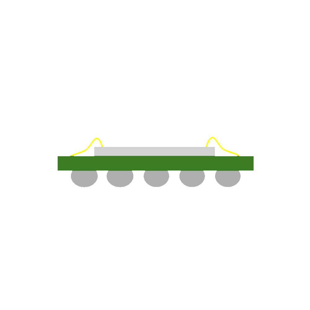
Wirebonding bare dies on a substrate and attaching balls
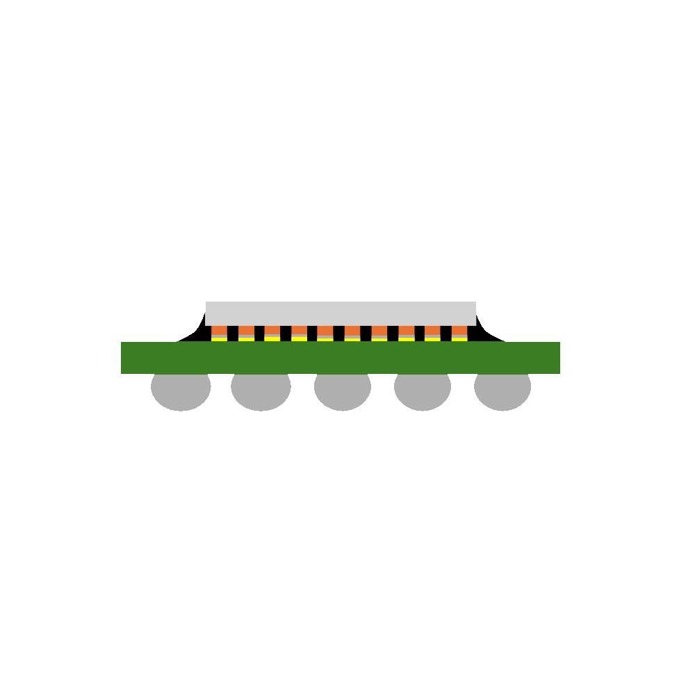
FlipChip attach to BGA substrate
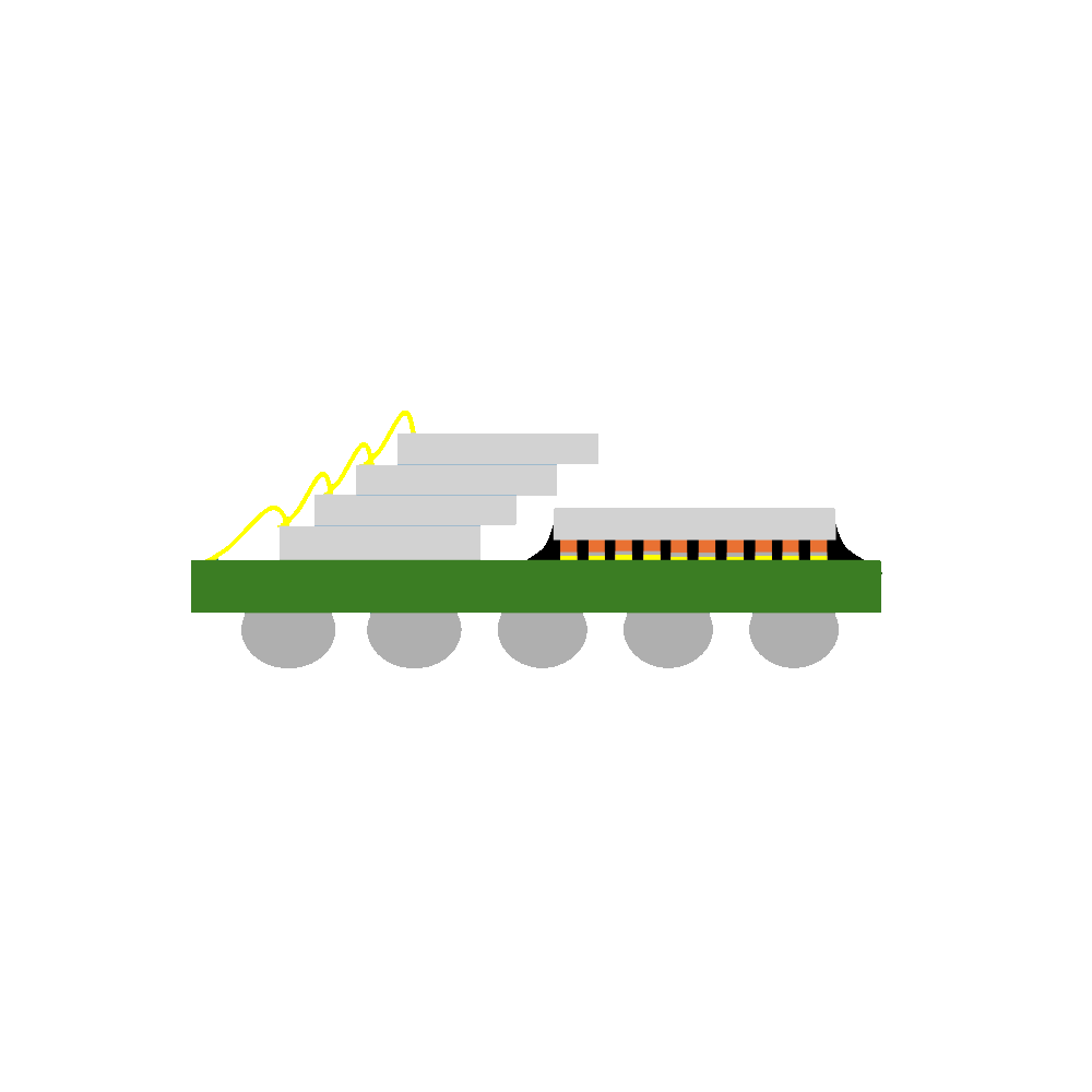
Combination of wire bond Dies and FlipChip packages
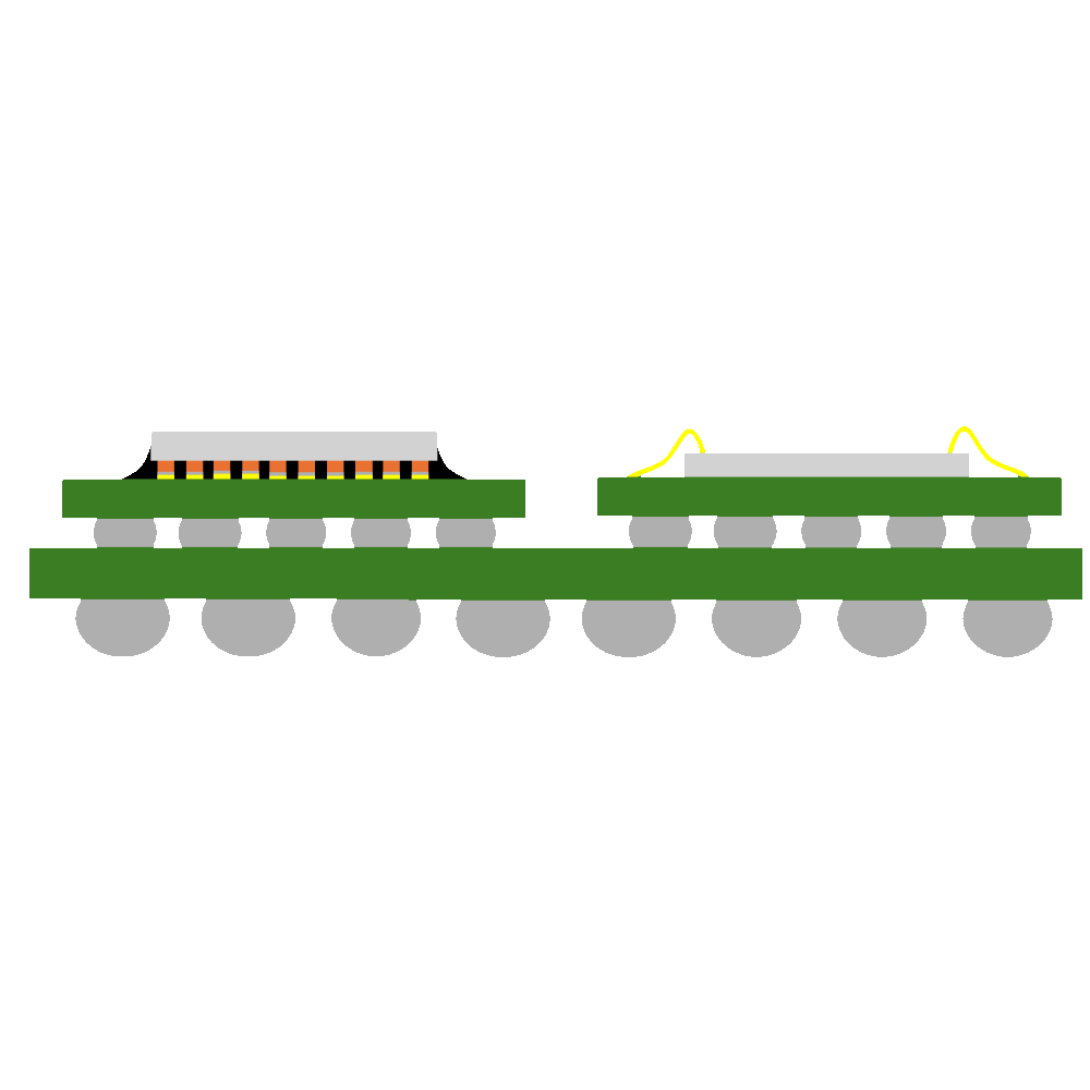
Combination of various substrates on a common carrier
Swissbit Products Featuring SiP Technology
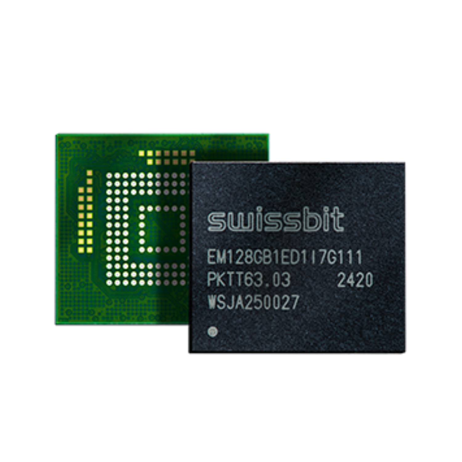
Swissbit's EM-30 e.MMC solutions demonstrate system in package integration at scale: NAND flash controllers and multiple NAND dies combined into compact 11.5x13mm to 14x18mm packages. Die stacking enables up to 256GB capacity with e.MMC 5.1 interface speeds while maintaining extended temperature operation (-25°C to +85°C). This vertical integration reduces board space requirements by 60% compared to discrete controller-plus-NAND implementations—critical for embedded systems, medical devices, and industrial IoT applications where PCB area directly impacts product size and cost.
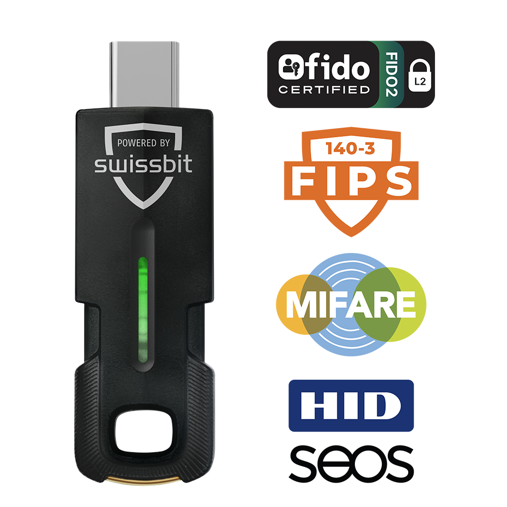
The iShield Key 2 showcases multi-technology system in package assembly: FIDO2-certified secure element, NFC controller, and physical access components integrated in a standard USB-A form factor. Side-by-side die placement optimises RF performance for contactless operation while fine-pitch wire bonding (40µm) connects all functional blocks to a compact substrate. Robust encapsulation protects sensitive components, enabling simultaneous passwordless authentication, encrypted communication, and building access—functionality impossible with discrete component approaches.
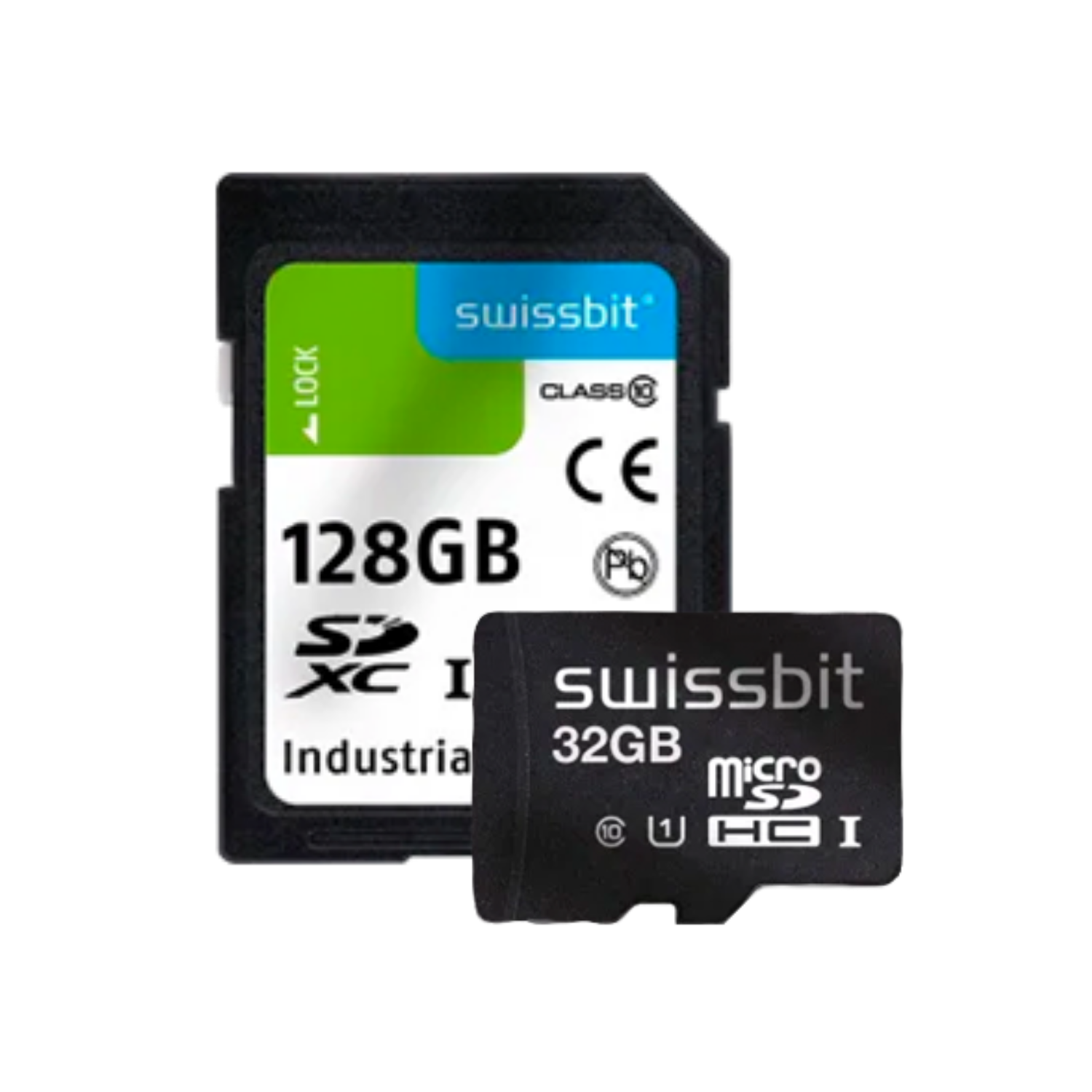
Swissbit's SD, and microSD memory cards leverage advanced packaging to achieve extreme miniaturization without compromising industrial reliability. Many products manufactured in Berlin integrate controller, NAND flash, and passive components into form factors as small as 11x15mm (microSD). System in package assembly enables extended temperature qualification (-40°C to +85°C), high shock/vibration resistance (up to 2,000G), and 10+ year operational lifetimes—specifications standard consumer cards cannot achieve.
Why Choose Swissbit for System in Package?
Many Swissbit products featuring SiP technology are manufactured at our Berlin facility under ISO 9001, IATF 16949, and ISO 27001 quality standards. This European manufacturing provides supply chain security and transparency increasingly important for defense, critical infrastructure, and automotive applications.
Swissbit controls the complete value chain from hardware design and firmware development through SiP manufacturing to final configuration. This integration enables optimized solutions: storage products engineered for industrial reliability, security modules combining multiple technologies, and customized packages meeting specific customer requirements.
Since 1995, Swissbit has developed specialized SiP expertise for industrial-grade electronics. This experience spans from first die stacking to current 16x NAND integration, security processor packaging, and custom solutions for OEM customers requiring specific form factors or configurations.
ISO9001 (Quality Management), IEC60068 (Industrial Temperature Testing), ISO27001 (Information Security), ISO14001 (Environmental), ISO50001 (Energy), REACH, RoHS, Conflict Minerals compliant
Frequently Asked Questions
Explore Swissbit SiP Capabilities
Ready to discuss how system in package technology can address your application requirements?
Our engineering team provides technical consultation.