Swissbit Blog
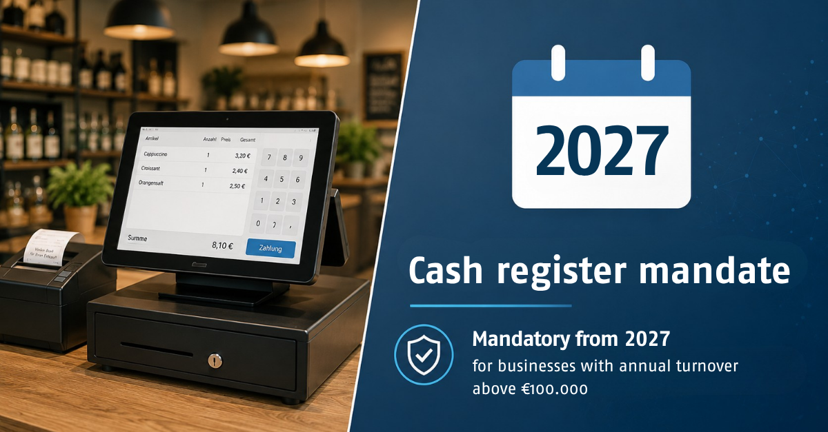
Germany’s planned 2027 cash register mandate could reshape POS strategy for retailers, hospitality businesses and service providers. This blog explains what may change, why TSE integration matters, and how certified hardware, cloud or hybrid fiscalization solutions can help build secure, audit-ready cash register environments in Germany for the years ahead.

Edge, networking and industrial systems need storage that delivers more than headline speed. The Swissbit A2000 Series combines PCIe Gen4 NVMe performance with industrial-grade reliability, consistent low latency, power-loss protection, security features and endurance options for real workloads in demanding environments.
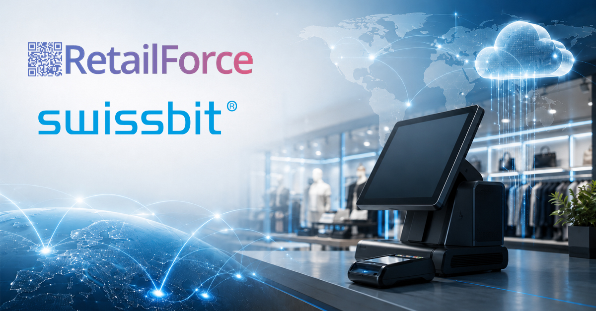
Fiscal compliance across borders does not have to be complicated. In this article, we explain how RetailForce and Swissbit are strengthening their collaboration – and why the combination of middleware and secure TSE technology helps companies implement fiscalization in a simpler, more scalable and legally compliant way.
Swissbit is expanding its industrial storage portfolio with advanced BiCS5 NAND technology. Learn how the new generation supports smooth migration, long-term availability, flexible endurance options, and cost-efficient designs across established interfaces and form factors.
Cloud-TSE, hardware TSE or hybrid fiscalization? Choosing the right approach is more than a compliance decision. It shapes POS architecture, rollout, maintenance, scalability and long-term life cycle management. This article offers a practical decision framework for finding the right TSE strategy for different POS and business environments.

In a volatile storage market shaped by allocation, price increases, and e.MMC discontinuations, long-term stability matters more than ever. Swissbit’s in-house manufacturing in Berlin, from wafer-level production to final testing, gives customers quality, flexibility, and supply chain control for embedded storage designs.

As AI, edge computing, security and compliance reshape infrastructure requirements, standard memory and storage products are no longer enough for many applications. In this blog, we explore why customization is becoming essential in 2026 and how tailored firmware, security, endurance, thermal behavior, pre-load services, labelling, packaging and other adaptations help turn standard compatibility into real application value.
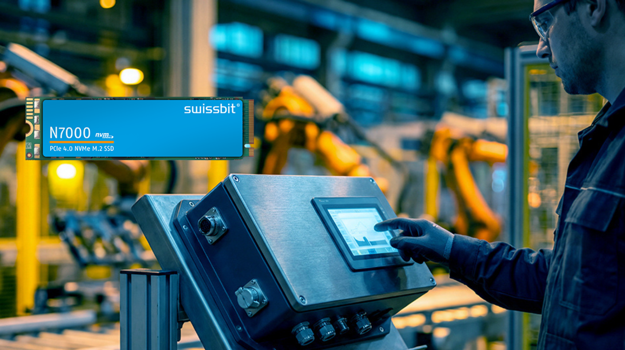
Embedded systems need more than peak SSD speed. This blog explores why modern industrial, networking, and edge AI applications require PCIe Gen4 storage that balances sustained performance, low power consumption, thermal stability, and long-term reliability — and how Swissbit’s N7000 series addresses these demands.
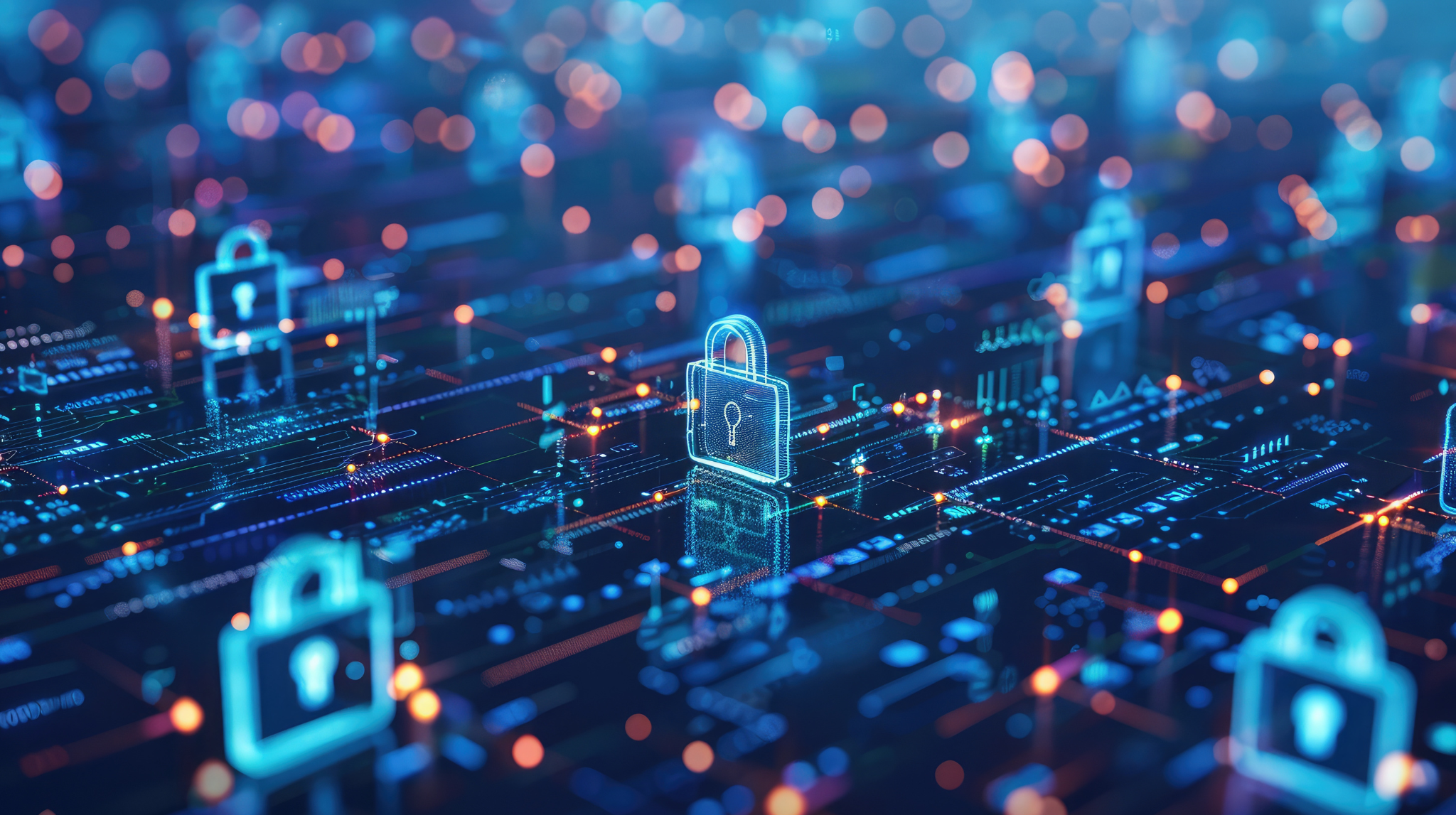
As industrial and embedded systems grow more connected, storage becomes a critical attack surface. This blog shows how Swissbit’s retrofit-ready Security Upgrade Kit helps protect credentials, configurations, and sensitive data in industrial equipment, drones, and embedded Linux platforms, strengthening system integrity, access control, and reliable operation without hardware redesign.

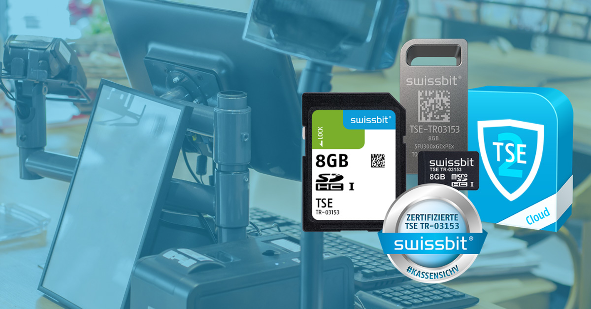
Learn what the German Cash Register Security Ordinance (KassenSichV) requires, who it affects, and how businesses can build a reliable, scalable POS compliance strategy with the right TSE approach.
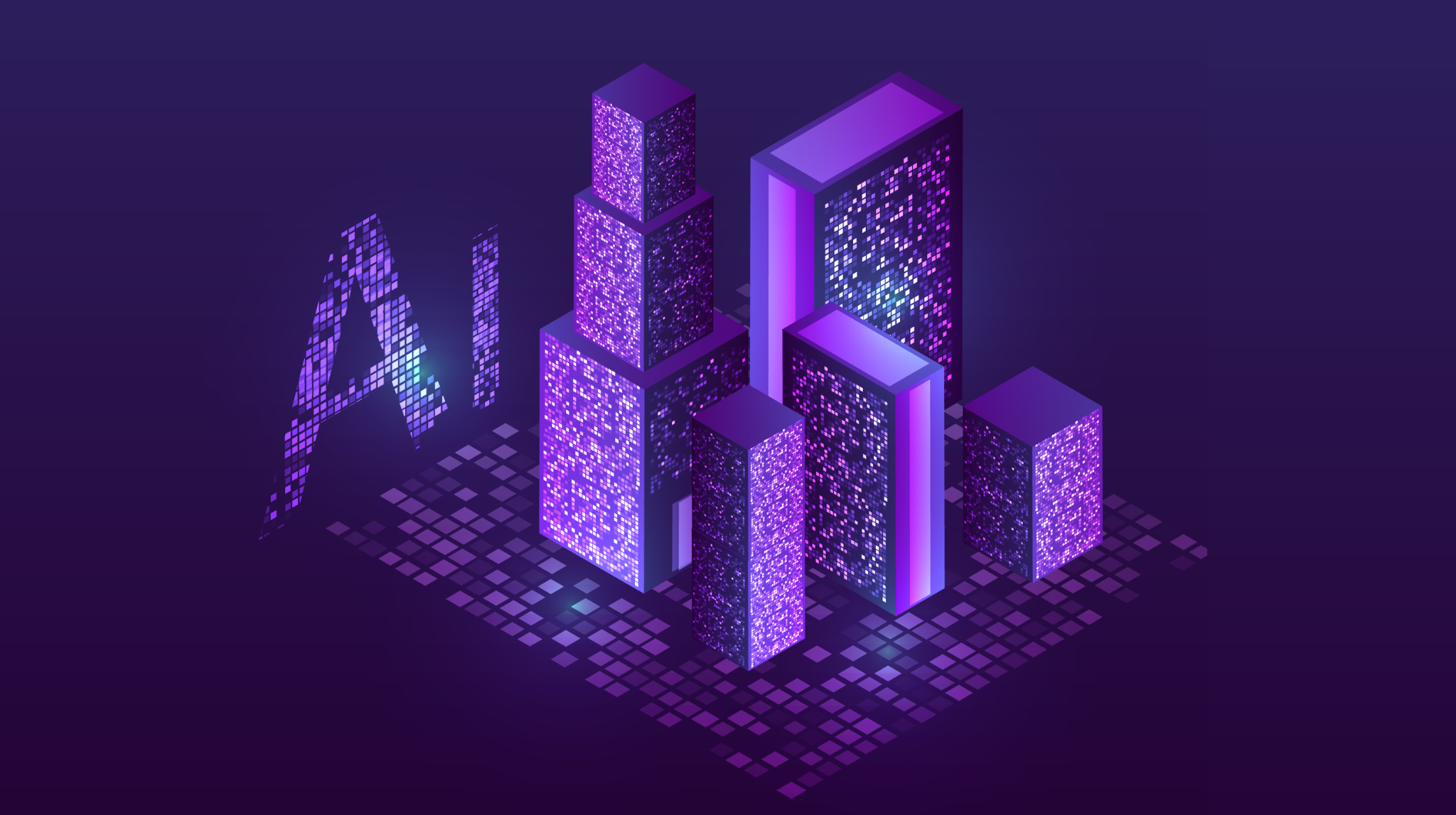
AI at scale is not just a software story. This blog explores how power, cooling, storage, and resilient supply chains are becoming the true enablers of AI infrastructure, and why long-term reliability, industrial execution, and ecosystem thinking will define who creates lasting value in the AI economy.

AI runs on more than GPUs and memory. Behind every model, industrial flash storage keeps boot processes, firmware, logs, telemetry, and edge inference systems reliable, secure, and available. From data center infrastructure to rugged edge servers, Swissbit helps build the stable, trustworthy foundation AI needs to perform in real-world conditions.
I’m excited to share that Swissbit is partnering with Pointsharp to strengthen European authentication security. With the iShield Key 2 now supported in Pointsharp’s IAM platform, we’re giving organizations even more flexible, future‑ready options for secure, passwordless access.